Home
Class E Overview and
Theory of Operation
Output Circuit Values & MOSFET ratings
High Power & Harmonic Reduction
Construction Overview
Simple 400 Watt
RF Amp for
80 meters
Using a lower power
transmitter as an
RF source (A to D converter)
Pulse Width Modulator and power supply
24 MOSFET RF Amplifier - Step by Step
Analog Modulator (Class H) and power supply
Overall Schematic of a complete modulator/power supply
![]()
.
Pulse width Modulator and Power Supply by WA1QIX The pulse width modulator design shown above can supply up to watts 450 watts (45 volts at 10 amperes) of modulated DC into a 4.5 ohm load. The particular modulator shown here will deliver a little over 400 watts (45 volts at 9 amperes), because that is the RF amplifier I was using at the time. The schematic diagram shows severl configurations of the modulator, for different power levels. The PWM (Pulse Width Modulation) generator board itself operates with line level audio. An adjustable negative peak limiter is included. The modulator can be configured (during construction) with up to 8 poles of audio filtering, and any cutoff frequency may be used. This filtering is very important to keep unwanted high frequencies (and harmonics of these high frequencies) from intermodulating with the PWM switching frequency, causing aliasing components to appear in the output. The implementation includes an "Efficiency Meter", an invaluable tool for tuning class E transmitters for optimum efficiency, and maximum RF output. This same circuit contains sophisticated overload detection and shutdown circuitry. Note: an oscilloscope is needed for construction and initial testing. The front panel is made with a plastic overlay. The overlay is comprised of 2 transparency (overhead projector) plastic sheets carefully taped together. An explanation of how to make the overlay is included in this document. Schematic List:These schematics are in PDF format, and should be viewable on virtually any computer. As a note, Adobe reader allows large pages to be printed on two pieces of paper, in two halves, allowing easy printing on two 8.5 x 11 sheets. These can then be joined together to form a single, large schematic that will be easier to read than if the whole diagram were confined to a single 8.5 x 11 sheet.Rev F Schematics and parts lists (most recent revision)
Rev D Schematics and parts lists (previous revision)
Rev C Schematics (previous revision) |
Circuit OverviewHow it WorksAudio is fed to the modulator at line level, directly to the input amplifier and phase select IC U200.
If microphone level audio is needed, a microphone preamp (available as
a kit), is used. The line level output of the microphone preamp is
then fed to the input of the PWM generator board.
To the right: A block diagram of the pulse width modulator showing most of the major components. The diagram and the modulator schematic use the same component identifiers (such as U300) to aid in understanding how the modulator works. |
|
From U200, the audio is fed to the negative peak limiter, and then into
the anti-aliasing audio filter implemented around a TL074 IC (U300). The
filter serves two purposes: 1) The filter prevents high audio frequencies, or
audio harmonics from mixing with the pulse width modulator switching
frequency (about 160kHz), and 2) The filter controls the audio bandwidth
of the modulator.
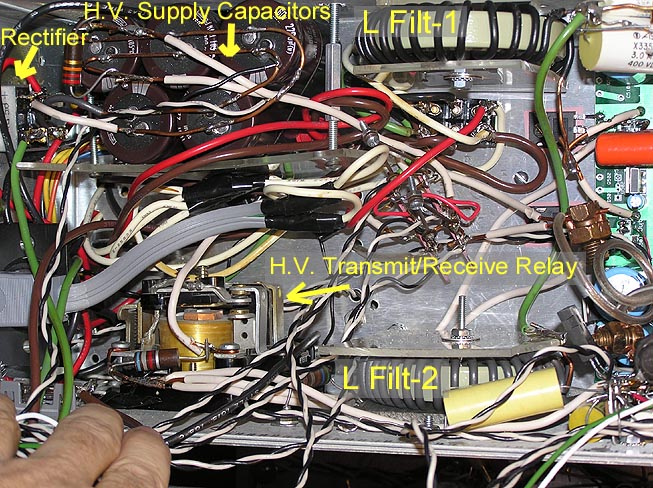
After the anti aliasing filter, the audio is fed into the PWM controller IC, a Unitrode UCC25701N. This is an excellent voltage mode PWM controller, and exhibits extremely linear characteristics, resulting in a very clean pulse width modulated signal. The IC also implements Feed Forward, by which a small sample of the high voltage power supply's ripple is fed to the PWM controller, out of phase. The controller essentially modulates the pulse train with the power supply's ripple - out of phase with the actual ripple, and the result is a cancellation of the power supply ripple in the output. This is very effective at almost completely eliminating power supply ripple and hum. From the PWM controller, the pulse width modulated signal is fed to a 74OL6010 opto isolator IC, U500. The isolation is necessary because the modulator is implemented as a source follower, and the driver IC along with other associated circuitry floats with the pulse width modulator output. IC U500 drives the IXDD414 (U502) driver IC. The driver IC drives the gates of the modulator MOSFETs The modulator MOSFETs Q500 - Q504 amplify the 12V signal from driver U502 up to the full power supply voltage. When the gates of the Q500 bank are driven positively (PWM input signal goes high), the MOSFETs turn on hard, conducting power from the 115V high voltage power supply connected to the MOSFET drains, through the MOSFETs, to the MOSFET sources and ultimately to the output filter. When the PWM input signal goes low, the gates of Q500 are driven low, and the MOSFETs turn off. Energy stored in the input inductor of the filter is released, and the voltage at this point drops very rapidly. This is the "flyback" effect. The voltage would fall WELL below zero if the damper diodes (D507 - D511) did not clamp the voltage at 0V, and conduct the energy back to the (negative side of) the power supply. The PWM output filter formed by, L FILT-1, L FILT-2, C FILT-1 and C FILT-2 integrates the pulse train (filters it out), and the filter output is modulated DC. |
Circuit and Construction Details
Note: these circuits can be implemented without the PC described boards. The boards make it somewhat easier to implement the low level circuitry, however dead bug or other breadboard construction can be used.
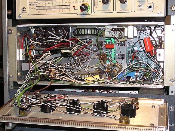
To the right: The pulse width modulator with the front panel open. The chassis including the front panel (without the meters) for this modulator was purchased at a local ham radio flea market for 50 cents, and was orginally used for another piece of equipment. Flea markets are a good source of parts for the home builder. Other sources are Ebay and various ham radio bulletin boards. |
PWM Generator Including Anti-Aliasing FilterThe PWM generator can be used with a wide variety of configurations, modulator designs and layouts. The PWM output is selectable, standard TTL or +12V, operating at approximately 160kHz. The outputs are low impedance, suitable for driving terminated, shielded cable.A feed-forward input and on-board adjustment is provided, and when used correctly will significantly reduce the effects of high voltage power supply ripple on the modulator output. The microphone preamp board is available. If used, the microphone preamp provides both amplification and power for a condenser microphone, audio processing (peak limiting/compression) and bass and treble (presence rise) adjustments. All necessary adjustments for proper pulse width modulator operation are provided on the board. Several optional external adjustment connection points are also provided, if the builder wishes to provide a front-panel adjustment for a particular function. The anti-aliasing filter can be configured with up to 8 poles. A single TL074 op amp is provided for the filter, and several filter configurations are shown on the schematics. How the filter is configured is up to the user. The 6 pole filter shown in the main schematic will yield very good audio quality up to about 6kHz, at which point the high frequencies will start to roll off. With 6 poles, there will be very little filter ringing. Two 8 pole filter configurations are also provided, giving a steeper slope to the high frequency roll off. Note that the resistors and capacitors used in the filter should be as close as possible to the values listed in the schematic. Precision resistors (1%) should be used. The exact values listed are standard precision resistor values, and are available from Mouser and other electronic component suppliers. The PWM Generator PC Board has the following inputs and outputs:

To the Right: Closeup of the PWM generator board and Efficiency Meter / Overload Shutdown board as installed in the modulator chassis. Note that all on-board adjustments are accessible, and the modulator can be operated and adjusted with the front panel open. Audio Inputs and Grounding Care should be taken to avoid ground loops and other problems in your implementation. The ground point at the audio input is usually connected to ground. It may be necessary to also ground the the board at the PWM output. A balanced input is provided on the PWM generator board, if required. The board may be configured to be either balanced or unbalanced. It is often desirable to provide an external audio level control. This is easily accomplished by simply connecting a potentiometer between the line level or microphone level input and the audio source. An audio phase select switch is provided on the PWM generator board. This switch is used to select the audio phase that results in the highest level of positive modulation. The PWM Output should be carried on a shielded (preferable) or twisted pair cable and must be terminated at the far end. Very long cable runs can cause high frequency roll off in the PWM waveform, causing integration of the waveform and subsequent distortion at the extremes of modulation. Rev. D of the PWM output board requires the +12V output from the PWM generator. Efficiency Meter / Overload ShutdownA second board (shown above) contains the Efficiency Meter and Overload Shutdown Circuitry. The board provides a variety of inputs and outputs, allowing the board to be used in many configurations and types of modulators.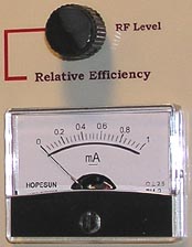
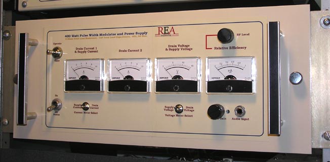
The overload sensing circuitry monitors both the current flowing to the RF amplifier and the corresponding modulator output voltage. This enables the overload system to more accurately monitor the power used by the RF amplifier. If the current used by the RF amplifier increases significantly more than the voltage applied to the RF amplifier, the system will detect an overload, and will assert two TTL outputs (overload High and overload Low) as well as open a DPDT relay. The relay can be connected to other parts of the circuit, such as the high voltage power supply. The TTL overload outputs are usually connected to the modulator low level circuitry, providing instant shutdown of the modulator output. This quick system shutdown is key to an effective overload protection system. The overload system also takes input from an optional external SWR bridge that provides around 1 or 2 volts DC from either the forward or reflected detectors. If the reflected voltage is more than about 1/2 of the forward voltage, the system will go into shutdown, and generate an overload shutdown event. The Efficiency Meter (Patent Pending) (Non commercial, individual use of the circuit and method permitted) is an innovative circuit that provides an effective and accurate method of tuning a class E transmitter. The meter compares the power input of the RF amplifier to the RF output and displays the result on a panel meter. The RF output voltage is generated by rectifying and filtering a small portion of the RF output. Tuning is simply a matter of obtaining the highest indication on the efficiency meter at the desired drain current. Since the RF output from the class E amplifier will change considerably as the optimum tuning point is reached, an RF level control is provided to keep the levels within the indication range of the meter. At optimum tuning, the meter will be sensitive to efficiency changes of under 1%. The Efficiency Meter / Overload Shutdown PC Board has the following inputs and outputs:
PWM Output Section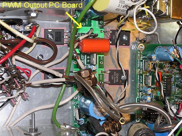 The PWM output PC board can be configured with as few as one (1), to as many
as five (5) power MOSFETs / Damper diodes. The number of devices installed
depends on how much power the system is required to deliver. Each modulator
MOSFET will handle about 250 watts of carrier power (DC input). So, if the
modulator is to deliver 400 watts carrier, two MOSFETs and two damper diodes
should be used.
The PWM output PC board can be configured with as few as one (1), to as many
as five (5) power MOSFETs / Damper diodes. The number of devices installed
depends on how much power the system is required to deliver. Each modulator
MOSFET will handle about 250 watts of carrier power (DC input). So, if the
modulator is to deliver 400 watts carrier, two MOSFETs and two damper diodes
should be used.
Since the peak current output from the modulator is very high, a number of modulator outputs and ground connections are provided on the board. At least two of these should be used up to 500 watts of carrier, and all output and ground connectoins should be used if possible. A #14 wire should be connected to each output and ground connection. At the output, these wires are joined together and ultimately connected to the input of the PWM filter. The ground connections should be returned to the chassis or ground with short leads. The board requires an 18VDC unregulated (and optionally unfiltered) DC input for the regulators supplying the optical isolator and for the charge pump that supplies a floating DC voltage for the the PWM driver IC (IXDD414). This 18VDC unregulated voltage should be supplied by its own power supply, and should not be taken from the PWM generator board or power supply. This is done to reduce coupling between the high power PWM output section and the highly sensitive low level circuitry on the PWM generator board. The high voltage DC input to the board should be switched on and off with transmit / receive. The capacitors on the modulator output board will normally remain charged between transmissions. A resistor should be placed across any relay that switches the DC from the power supply to the PWM output board to minimize relay arcing when going from receive to transmit. This is customarily part of the main power supply and transmit / receive circuitry (see transmit / receive circuit diagram). |
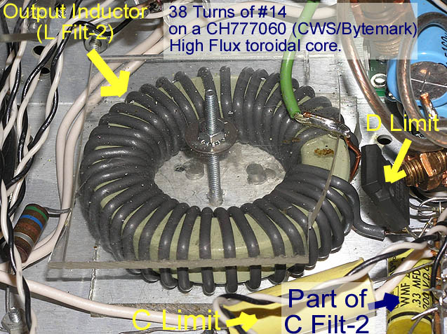
The PWM Output Filter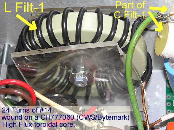 The output filter is one of the most important components in any PWM system.
While the design and construction of the filter is not particularly difficult,
and improperly designed or implemented filter can be the cause of major problems.
All of the filters shown here are Butterworth filters. This filter implementation
gives a good cutoff characteristic, without too much ripple (bumps in the
response) in the passband of the filter. Each reactive element (inductor or
capacitor) results in one filter pole. A 4 pole filter is used here.
The output filter is one of the most important components in any PWM system.
While the design and construction of the filter is not particularly difficult,
and improperly designed or implemented filter can be the cause of major problems.
All of the filters shown here are Butterworth filters. This filter implementation
gives a good cutoff characteristic, without too much ripple (bumps in the
response) in the passband of the filter. Each reactive element (inductor or
capacitor) results in one filter pole. A 4 pole filter is used here.
This particular pulse width modulator implementation is designed for a 5 ohm load. This means that the RF amplifier is adjusted such that it always represents a 5 ohm load to the modulator. As an example, if the modulator (at carrier) is delivering 40 volts DC, the RF amplifier current must be adjusted to be 8 amperes. This yields a load of 5 ohms - [40V / 8A = 5 Ohms]. If the modulator output were 45 Volts, the RF amplifier current would need to be 9 Amperes to maintain the 5 ohm load on the filter. |
|
.
.
 Inductor Construction
The input and output inductors of the PWM output filter are wound on CH777060 High Flux Cores (CWS/Bytemark). These cores are designed to be very stable over large variations in current, and are also very good when used with a high DC bias. The inductors are wound using #14 insulated, solid copper wire. The turns should be spaced evenly around the cores, so as to utilize as much of the core as possible. In this implementation, the PWM filter inductors are held in place between 2 pieces of plexiglass. The filter inductors generate very little heat, so any convenient method of mounting may be used. The inductors should be sufficiently separated from each other to prevent coupling between the inductors. These inductors are usable up to about 9 amperes of modulated DC. Above that, a larger core, or stacked cores should be used to prevent core saturation. An air core inductor may also be used. Capacitors used in the Output Filter The capacitors used in the output filter (C Filt-1 and C Filt-2) should be as close as practical to the values specified by the filter design. Use smaller capacitors in parallel to get the proper value if necessary. The leads from the capacitors in the filter and the ground plane should be as short as possible. Any stray inductance in the capacitor leads will reduce the effectiveness of the filter. The capacitor voltage rating should be at least equal to the high voltage power supply output voltage. When figuring the capacitance of the last capacitor in the filter, be sure to include the capacitance of RF bypasses and any other capacitance that may exist between the filter and the load. The actual value of the output capacitor is the sum of all of the bypass and other capacitance in the circuit. This is often overlooked, and the result will be too much capacitance in the filter output capacitor. Designing a Different Filter If you are designing a modulator to work into other than 5 ohms, or if you want a different cutoff frequency, or if you want more poles (sharper cutoff slope), you will need to design your own filter. The process of designing the output filter is fairly straight-foward. Assuming you are using a Butterworth filter, there are plenty of Butterworth filter calculators available on the Internet to aid you in your design. You can also use the filter tables found in the ARRL handbook and other similar publications. Once you have the values for the inductors and capacitors needed for the filter, construction is simply a matter of winding the coils (whether toroidal or air wound) and connecting individual capacitors in parallel (if necessary) to get the needed circuit values. Wire Size The wire size used in the filter, and in the interconnecting wiring should be sufficiently large to carry the peak output from the modulator without introducing too much voltage drop. #12 or #14 wire works well up to about 9 amperes of unmodulated DC (carrier) current, #8 or #6 should be used with filters carrying up to about 15 amperes of unmodulated DC. Using Air Wound Inductors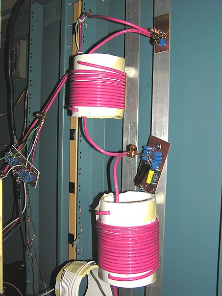 Air wound inductors work very well, and there are no core saturation issues with
which to contend. Air inductors are also, in general, quite a bit less expensive
to construct. The primary disadvantage of an air wound inductor is the size.
More wire will be necessary to achieve the desired inductance than would be
required in the same value inductor constructed on a toroidal core.
Air wound inductors work very well, and there are no core saturation issues with
which to contend. Air inductors are also, in general, quite a bit less expensive
to construct. The primary disadvantage of an air wound inductor is the size.
More wire will be necessary to achieve the desired inductance than would be
required in the same value inductor constructed on a toroidal core.
Since the amount of wire used in a typical air wound inductor can be significant, on the order of 10 to 20 feet, the inductor should be wound on some kind of form. PVC pipe works very well for the purpose, and it is easy to obtain, and is not at all expensive. It is also easy to drill. For large inductors, schedule 40 PVC should be used. It is usually easiest to lay the wire out on the floor, and carefully roll the PVC over the wire, keeping it tight while doing so. Some tape or glue can be used to hold the wire in place if there is a possibility of movement on the coil form. To the right: PWM output filter implemented using air wound inductors. Note the capacitors built up by using multiple smaller capacitors in parallel to obtain the proper values. #6 wire is used in the filter inductors and in all interconnect wiring. |
Power SupplyTypically, a single voltage output power supply is all that is required for a pulse width modulator. The power supply voltage requirements will depend on the final RF amplifier carrier level voltage requirements. Generally, at least 2.5 times the carrier level DC voltage is required. Example: A transmitter operating at 45VDC, carrier level, using a pulse width modulator, will require a power supply voltage of at least 113 volts. 120V would be better, as there is usually some small voltage loss in wiring, modulator MOSFETs, etc.
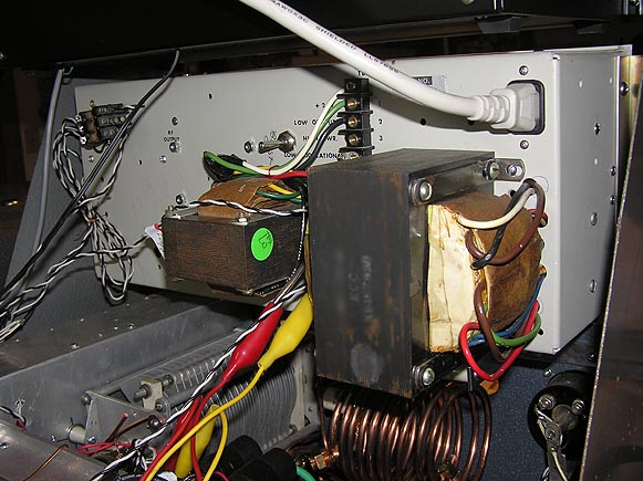
To the Right: Power Supply section of the pulse width modulator. The filter is made up of 5 2200uF 160V electrolytic capacitors. The high voltage transmit/receive relay can be seen at the bottom of the chassis. The internal power plug and outlet (visible to the far left) is provided to allow the connection of a Variac to the power supply, should it become necessary. It is a good idea to provide some facility for connecting a Variac to the high voltage power supply. The current rating of the supply can be calculated by taking the carrier level DC input to the RF amplifier, and dividing this by the efficiency of the modulator (usually better than 90%) to get the total power input required. The power input is then divided by the total power supply voltage, to get the DC current requirement. As an example, an RF amplifier operating at 45 Volts, 11 Amperes is using 495 watts of power (input). Figuring a modulator efficiency of 90% (which is probably low), the total DC input required will be 550 watts. Keying the Power Supply (Transmit/Receive) The transmit/receive system for the transmitter should not allow the high voltage power supply T/R relay to be activated until all other relays or systems have been activated and had time to "settle". The power supply T/R relay should also be connected to the overload protection relay on the Overload Protection PC board, or some other overload shutdown system. When going to receive, the power supply T/R relay should be the FIRST relay to be deactivated. Ideally, the pulse train should be stopped slightly before or at the same time that the power supply T/R relay is deactivated. This will immediately stop the modulator output, and quickly remove power from the RF amplifier. Filter Capacitor The modulator uses a capacitor input filter consisting of 5 2200uF, 160V electrolytic capacitors in parallel giving a total capacitance of around 11000uF. This is not a huge amount of filter capacitance, and there will be a small amount of ripple on the output. This small ripple can be almost completely eliminated by using the Feed Forward feature of the PWM generator. The Power Transformer
To the Right: Back of the modulator / power supply showing the power transformer in the foreground, and a 10VAC, 8A "boost" transformer behind it. The power transformer costs $24.00. I currently have some of these transformers available. Contact me if interested. The boost transformer is an old filament transformer (10V @ 8A) I got at a flea market for $3.00. The power transformer used for this modulator delivers approximately 88VAC at 5.5 Amperes. This will yield a DC voltage of approximately 112 to 115 VDC, under load, depending on line voltage. The transformer secondary is center tapped, facilitating a "tune" position, facilitating transmitter tune up at low power. In this modulator, a switchable 10VAC Boost transformer is included. The secondary of the Boost transformer is connected (when switched into the circuit) in series with the secondary of the main power transformer, boosting the total secondary AC voltage by 10 V. This will add appximately 12 to 13 VDC to the rectified and filtered output. |
Making a Front Panel Graphics OverlayThe front panel of my implementation is made with a plastic overlay. The panel could also be made using dry transfer lettering, modern labels or other types of decals.The overlay is comprised of 2 transparency (overhead projector) plastic sheets carefully taped together. Use a graphics program such a Adobe Photoshop (I used Photodelux - a watered down version of Photoshop) to create the graphics, text, etc. for your overlay. Then reverse (flip horizontally) so the image is backwards, and print it on the transparency plastic. By printing in this way, you will be looking through the overlay at the ink, and the ink will be on the inside, protected from scratches. If you must use more than one sheet, be sure to have an inch or two of overlap between the two halves of the overlay. Tape these one over the other, and then carefully cut BOTH pieces of the overlay at the same time, in the overlap area. It will then be relatively easy to join the two pieces and have a very clean seam. Use thin transparent tape (on the back) for this purpose. Getting the Background Color Most printers will not lay down sufficient ink to make a "flood" (the solid background color of the panel and overlay). There are several ways to get a solid background. If the panel is very clean (no holes or other visible blemishes), you can simply place your overlay directly over the front panel that is painted with the background color. If the panel is not sufficiently clean to use this method, you can use a piece of thin metal or paper painted with the background color and put the overlay over this. You can also spray paint the back of the overlay, over the ink. Special paint must be used, as most spray paint will not adhere well to plastic. Even with the correct paint, there is still a danger of the paint peeling off the back of the overlay, so observe care when handling a painted overlay. Allow sufficient time for the paint to dry before handling the overlay. Do not rub against the front of the overlay until it is resting against a solid surface. Once in place over a solid surface, a back-painted overlay should hold up well.
More Information about Pulse Width ModulatorsMore information about Pulse Width Modulators, and how the PWM Modulator works can be found in my Solid State PWM article. |

 Most of the low level circuitry, along with the PWM output section is
implemented on three printed circuit boards. The first board consists of
the PWM generation circuitry, input filter, negative peak limiter. An optional
microphone pre-amp, with compressor and tone controls is also available.
The PWM board contains its own power supply (using an external power transformer)
that also supplies power to the Efficiency Meter / Overload Shutdown board.
Most of the low level circuitry, along with the PWM output section is
implemented on three printed circuit boards. The first board consists of
the PWM generation circuitry, input filter, negative peak limiter. An optional
microphone pre-amp, with compressor and tone controls is also available.
The PWM board contains its own power supply (using an external power transformer)
that also supplies power to the Efficiency Meter / Overload Shutdown board.